
In an industry where nanometer-scale precision defines success, advanced semiconductor metrology plays a critical role in enabling technological progress across electronics, mobility, energy, and digital infrastructure. The demand for continuous product development requires precisely controlled manufacturing processes that can be established by rapid and accurate metrology solutions – optimizing productivity while minimizing resources and risks. Through our state- of-the-art measuring systems and research work, Semilab contributes to the technological progress of the world.
Semilab in a nutshell: Academic excellence to the industry
SEMILAB is a strategic supplier of state-of-the-art metrology solutions to leading wafer manufacturers, IC device makers in
the More-than-Moore market segment, solar and display industries worldwide, based in Hungary with R&D and product centers and a network of representatives in Europe, the USA and across Asia.
What began as a small, research-driven company, founded in 1989’s Hungary, has evolved into an essential global supplier
of measurement and characterization solutions, while also actively contributing to collaborative EU-funded research projects that shape the future of European and global semiconductor innovation. We have inherited a strong academic background from the founders of Semilab – who were physicists and engineers from the academic research and were finding the path for their innovations in the semiconductor industry. This still inspires the growth of our colleagues’ scientific expertise and helps to implement our 30+ years of know-how into building measurement equipment.
Innovation in the DNA
Semilab’s journey reflects how deep scientific expertise, continuous innovation, and strategic growth can transform the vision of a handful of scientists into a key player in the worldwide high-tech ecosystem. Today – because of the extensive amount of R&D work and the acquisition of suitable assets and technologies – Semilab designs, produces, and sells metrology solutions for the characterization of semiconductor and photovoltaic materials, for monitoring the manufacturing process of semiconductor devices, flat panel displays and solar cells, and for R&D purposes in these areas.
Our own unique inventions and original technology research keep us continuously developing our products and making
innovation the basis of our metrology expertise.
Semilab’s growing portfolio offers more than 300 configurable metrology solutions of 45 product lines, based on optical and
electrical measurement technologies for testing, verification and monitoring of various materials. As an innovation hub, working with over 200 physicists, Semilab is ready to join the scientific movement bringing forward the European semiconductor scene, by utilizing its long-term scientific research and RDI in projects aiming to elevate the power
electronics, photonics, 3D-RAM, advanced logic (CFET), heterogeneous integration or advanced packaging and 5G/6G markets.
European leader in metrology & inspection equipment
Semilab is committed to enabling stable and long-term operation of manufacturing or quality control processes of its industry partners, whether achieved through mature technology or a unique development.
Semilab offers an extensive metrology portfolio covering key monitoring steps in semiconductor manufacturing, including
SRP for spreading resistivity profiling, WT/ DLTS for purity and bulk contamination checks, and EIR for oxygen and carbon
content measurements. Semilab positions its automated atomic force microscopy (AFM) system also to the wafer maker
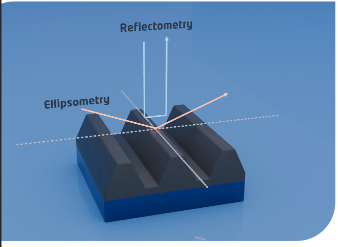
market to characterize surface roughness of the produced bare wafers. Due to various acquisitions, the company holds a strong market share in epi wafer characterization, from resistivity and doping measurements using mercury contact CV (MCV), air- gap CV (ACV), QC, and SRP, to epi layer thickness with large-spot FTIR (EIR), Model- Based Dimensions (MBD) for geometric characterization of periodic structures such as SiC trenches, and Raman spectroscopy for precise stress measurement and crystalline quality evaluation of advanced Si-based structures including SiGe, sSOI, and GeOI,
enabling accurate process control in next- generation logic device manufacturing.
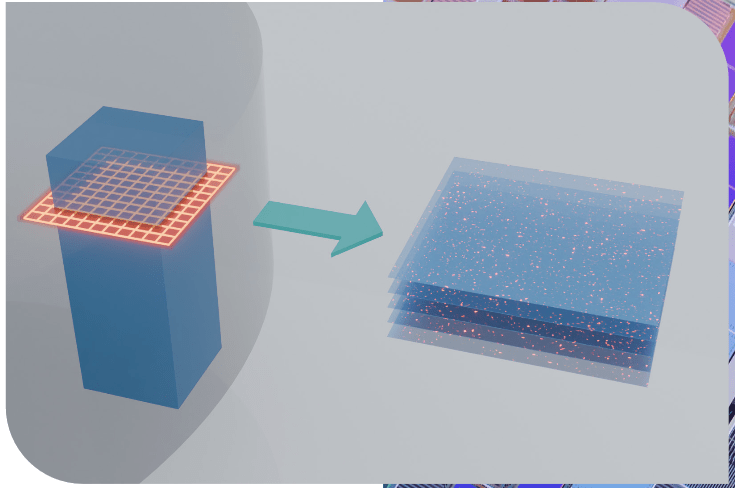
Semilab also offers metrology solutions for epi defect characterization via polarized stress imaging (PSI), lifetime measurements using WT, and ion implantation dose metrology before activation and annealing with photomodulated reflectivity (PMR). Its photoluminescence-based techniques, including the EnVision (Enhanced Vision) system, detect buried defects such as dislocations, oxygen precipitates, or stacking faults that are invisible to conventional optical
inspection. Supporting these capabilities, Semilab operates in-house cleanroom and lab testing facilities for joint R&D&I projects and offers university courses and training directly in its labs.
Experienced with EU projects
Semilab places strong emphasis on close cooperation with customers, industrial partners, and leading European research
institutions to jointly address emerging technological challenges. The company is an active participant in numerous international R&D collaborations and EU-funded projects, contributing to the advancement of next-generation semiconductor and photovoltaic technologies, including silicon (Si), silicon carbide (SiC), and advanced PV applications. Its involvement spans initiatives focused on upgrading manufacturing processes, strengthening the European advanced packaging ecosystem, and driving progress in equipment and materials development, packaging design, simulation, testing, metrology, and failure analysis. In addition, Semilab contributes to projects centered on Industry 4.0 solutions, digital nano-characterization technologies, and innovative image sensor developments that enable the future of 3D imaging.
Semilab’s commitment to collaborative innovation is further reflected in its ongoing partnerships with leading European research institutes. In cooperation with Fraunhofer IISB, the company has established a joint research laboratory focused on wide bandgap materials, including SiC, GaN, and AlN, supporting next-generation power and high-performance semiconductor technologies.
In its joint work with Imec, Semilab contributes to advanced logic and memory development, with a strong focus on SiGe metrology using its photoluminescence based non-contact measurement systems. Meanwhile, collaboration with CEA-Leti
centers on strained SOI technologies, where the company’s Raman spectroscopy solutions enable precise material
characterization. In 2025 alone, these and other research collaborations resulted in 98 publications, including 27 peer-reviewed scientific articles.
Within these collaborative frameworks, Semilab leverages its extensive metrology expertise to deliver tangible results. The
company has deployed state-of-the- art measurement systems for sample monitoring, developed integrated metrology
setups, advanced in-line and automated metrology solutions, and expanded the boundaries of existing technologies to
create novel measurement environments. Its contributions are supported by high- resolution, high-throughput imaging-based infrared inspection systems, imaging photoluminescence tools, advanced optical metrology platforms, atomic force
microscopy, and Raman spectroscopy solutions. By combining proven technologies with continuous innovation, Semilab not only supports the objectives of current projects but also contributes to shaping the future of semiconductor manufacturing. Building on its experience in collaborative research environments, the company looks forward to
further opportunities for joint development, where shared expertise and coordinated innovation can continue to advance metrology capabilities and strengthen the broader high-tech ecosystem.
Partnership for future-forward metrology solutions
Looking ahead, Semilab remains focused on advancing metrology solutions that address the increasing complexity of
semiconductor materials and device architectures. The company places strong emphasis on expertise, long-term
commitment, and continuous research and development executed with the highest level of precision. Strategic priorities include void detection in advanced packaging and heterogeneous integration; wide bandgap material and device characterization; SiGe device analysis; photonics defect control; and quantum material characterization. In parallel, Semilab is strengthening AI-based defect classification for Si and SiGe epitaxial multilayers, enhancing industrial application know-how across critical process parameters, developing robust analytical methodologies for key epitaxial properties, and expanding characterization libraries for advanced 2D and 3D device structures.
Recognizing that shared knowledge and coordinated expertise drive Europe’s technological progress, Semilab, a strategic
supplier of state-of-the-art metrology solutions to leading wafer manufacturers, IC device makers in the More-than-Moore segment, as well as the solar and display industries worldwide, remains committed to collaborative innovation that addresses the semiconductor challenges of today and tomorrow.