

Written by Dr. Dirk Schumann / Research Fab Microelectronics / Published on June 24, 2026
In advanced microelectronics, the competitive edge is no longer defined by individual technologies, but by the ability to integrate them into reliable, scalable systems. As chiplet-based architectures and heterogeneous integration become the new standard, the key challenge lies in translating fragmented capabilities into coherent production flows. The APECS Pilot Line addresses this shift by placing demonstrators at the center of its approach: not as showcases, but as integration testbeds that validate how technologies interact under real industrial conditions and ultimately deliver measurable system-level performance.
Europe’s ambition to strengthen its microelectronics ecosystem increasingly hinges not only on mastering individual
technologies, but on the ability to combine, integrate, and validate them at system level. As heterogeneous integration, chiplet-based architectures, and advanced packaging continue to reshape how electronic systems are designed and manufactured, the critical bottleneck is no longer access to single process steps, but the functionality of entire production chains across technologies, sites, and disciplines.
This is precisely where APECS – the European Pilot Line for Advanced Packaging and Heterogeneous Integration for Electronic Components and Systems – positions itself. Rather than focusing on a single technology or fabrication node, APECS has been conceived as a pan-European integration platform: bringing together distributed expertise, advanced infrastructure, and system-level design methodologies to enable next generation heterogeneous integration systems.
A pan-European pilot line built for integration
APECS is structured as a decentralized pilot line, pooling the technological capabilities of ten partners across eight European countries. Its foundation lies in the recognition that next-generation electronic systems, spanning high performance computing, photonics, radio frequency, sensing, or safety-critical applications, cannot be realized within
isolated process silos. Instead, they demand seamless interaction between materials, components, design flows, and production environments.
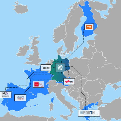
Figure 1: APECS Consortium: Germany (Fraunhofer-Gesellschaft as coordinator, FBH, IHP), France (CEA-Leti), Belgium (imec), Finland (VTT), Austria (TU Graz), Greece (FORTH), Spain (IMB-CNM, CSIC) and Portugal (INL).
What makes APECS distinct from other pilot lines is this explicit focus on integration rather than fabrication alone. Building on the infrastructure of the Research Fab Microelectronics Germany (FMD), APECS connects multiple specialized cleanrooms and process lines into a coherent, end-to-end production environment. A manufacturing execution system (MES) ensures consistency and quality across sites, while a central one- stop-shop-office (OSSO) coordinates access,
requirements, and solution pathways for industrial as well as academic users.
In doing so, APECS reflects a shift in how technological value is created in microelectronics: away from isolated technological advancements and toward co-optimized systems, where design, packaging, testing, and reliability are addressed collectively.
Technological scope: beyond classical advanced packaging
At the technological core of APECS lies a comprehensive platform for 2.5D and 3D heterogeneous integration, encompassing an unusually broad range of component technologies. These include CMOS, SiGe (BiCMOS) and as well as III–V-based devices for radio frequency, photonics, sensing, and emerging mixed-signal applications. Rather than treating these technologies as parallel options, APECS aims to combine them within shared architectures, enabling new system concepts that go beyond established packaging standards.
This ambition is reflected in four tightly linked technological focus areas:
- Quasi-Monolithic Integration (QMI): integrating multiple semiconductor functions into a single, compact solution without requiring all components to be fabricated on exactly the same silicon die or process node.
- Chiplet integration platforms: supporting both 2.5/3D integration technologies and allowing flexible assembly of modular, application-specific systems.
- Characterization, testing, and reliability (CTR): a holistic approach that combines characterization and testing as well as key innovation for safety and functional reliability, enabling continuous validation across the production chain.
- System-Technology Co-Optimization (STCO): a design framework that explicitly connects system requirements with technology choices, process flows, and manufacturing constraints, resulting in faster, more cost-effective, high- performance solutions for next-generation semiconductor products.
Together, these focus areas address a central challenge in advanced packaging: Ensuring that heterogeneous systems are not only technically feasible, but manufacturable, reliable, secure, and scalable.
From technology modules to system performance
A defining feature of APECS is that its technological focus areas do not exist in isolation. Development in QMI, chiplet platforms, CTR, and STCO are continuously aligned with system-level integration goals.The intent is not to optimize individual process steps, but to understand how decisions at
one stage, materials, interconnects, layouts, or assembly, affect performance, yield, and reliability across the entire production chain. This approach is particularly relevant for chiplet-based systems, where interfaces exist not only at material and electrical level, but also in design data, testing strategies, and logistics. By explicitly addressing these interfaces, APECS creates a framework in which gaps, risks, and trade-offs become visible early, long before technologies are transferred to manufacturing.
In practical terms, this means that technological progress within APECS is measured not only by process maturity, but by
how well different elements can be combined into functioning, repeatable system flows.
The crucial role of demonstrators within APECS
This systemic perspective explains why demonstrators play a central role within APECS. They are not conceived as showcase end products, nor as isolated proofs of concept. Instead, demonstrators serve as integration checkpoints – vehicles through which the full pilot line is exercised, tested, and refined. To this end, four demonstrators are being developed within APECS to identify interface incompatibility, process gaps, and data-flow issues that would remain otherwise hidden.
These demonstrators are designed to validate the achievements of the technological developments across multiple application domains. Each of the four demonstrators addresses a key field of the APECS pilot line. In doing so, they make use of the pilot line’s decentralized structure and its STCO framework to assess how technologies can be jointly deployed across distributed infrastructures.
A particular focus lies on the logistical and technological interfaces between different cleanroom environments, each with its
own requirements, as well as on enabling designers to access and combine diverse technologies. The objective is not only to optimize the transfer between individual process steps, but also to enable new process combinations that extend the capabilities of chiplet technologies and heterogeneous integration, while maintaining efficiency levels comparable to a centralized production environment.
Equally important, demonstrators establish a shared reference point for interaction with industry. They ground discussions with industrial stakeholders in observable system performance rather than abstract capabilities, while creating a feedback loop to identify and transfer requirements of new applications to the technological roadmap. For industry and investors alike, demonstrators provide tangible evidence of performance, reliability, and application relevance making the integrated capabilities of the APECS pilot line both visible and accessible.
In this way, APECS functions as a bridge between technological capability and system- level integration. Its core strengths – ranging from quasi‑monolithic and 2.5/3D integration, chiplet design platforms and advanced characterization, which all is enclosed by STCO – provide the new technological backbone for Europe.
Demonstrators as integration frameworks
Four demonstrators are developed within the APECS pilot line, each addressing different key challenges in microelectronics:
- The High-Performance Computing (HPC) demonstrator evaluates System- Technology Co-Optimization (STCO), where customer requirements such as cost, size, and energy consumption are built directly into chiplet and chip design e.g. for data center or edge AI solutions.
- The Multi Materials Sensor (MMS) module showcases the modularity of chiplets by integrating diverse sensors such as gas sensors, optical, and acoustic systems, while managing different thermal expansion, heat dissipation and cross interference.
- The Photonic Integration (PI) demonstrator focuses on edge InP technologies and photonic wire bonding to increase bandwidth and reduce energy consumption, addressing the growing demand for high-speed data transfer in compact systems.
- The Radio Frequency (RF) demonstrator will show innovative solutions for both wireless data communication and radar applications. The focus is on enhancing performance by combining the advantages of various semiconductor technologies, which are integrated using advanced heterogeneous integration techniques.
Rather than functioning as prototypes of end products, they serve as platforms to validate chiplet-based process chains across the pilot line. Together, these demonstrators show how APECS addresses the complexity of future microelectronic systems by developing optimized, scalable, and reliable solutions.
High performance computing (HPC) demonstrator
The accessibility to design and manufacture customer-tailored systems for High Performance Computing (HPC) and edge AI applications is extremely limited in Europe. While most of the required services are individually available within Germany, they widely lack an incorporation into a holistic solution’s landscape. The pilot-line’s HPC demonstrator implementation will take a subset, leveraging System-Technology-Co- Optimization (STCO) to build two chiplet- based modules for Data Center and Edge AI systems.
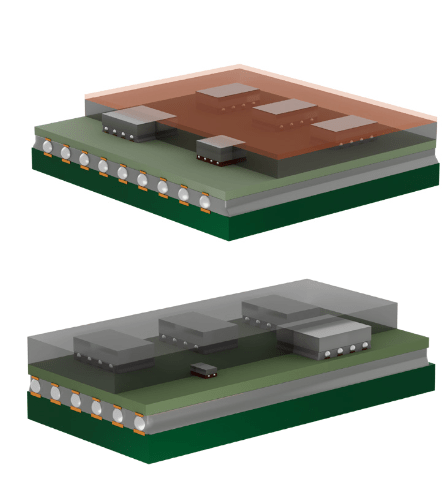
Figure 2: Conceptual illustration of chiplet- based modules for Data Center with heat sink on top (left) and Edge AI systems
without heat sink (right).
STCO is about integrating already available services such as
- system design for high-density integration, considering available standards like UCIe –S and BoW for chiplet-to-chiplet interconnections and new solutions
- System-on-chip (SoC), chip and chiplet design modelling and simulation of the physical module implementation, assembly, and physical integration of the modules
- module/system test and validation
These services are meshed together and completed by others to enable a seamless
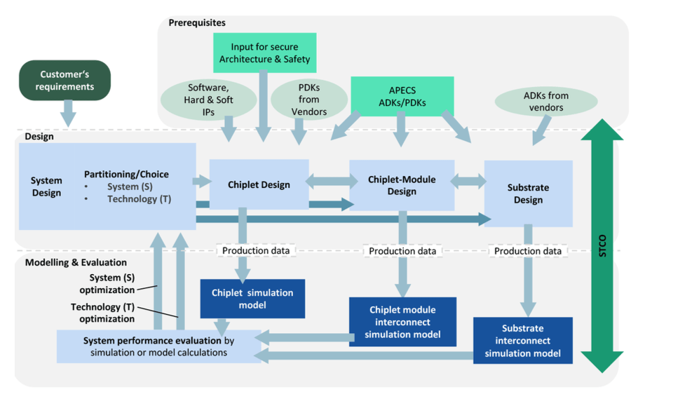
Figure 3: Sketch of the part of the holistic APECS System-Technology Co-Optimization (STCO) process that applies to the design of the HPC demonstrator modules.
and concurrent interoperability, to fill integration gaps and overcome interface challenges within the full production chain,
both at the material and data levels. For customer projects the pilot line will also offer reliability & product qualification. Eight Fraunhofer-institutes are involved in this demonstrator in chiplet architecture specification, fabrication as well as test,
packaging development, interposer and assembly developments: IIS & AISEC, IZM, IZM-ASSID, IPMS & FHHG IIS, IIS EAS & AISEC.
The STCO process is required to provide valid solutions with reasonable effort. The main reasons are:
- The partitioning and technology choice decisions interfere with each other in terms of system performance and budgetary implications as well as manufacturability, market and supply chain considerations, since optimizing only one after the other will not find an adequate solution.
- Changes in technology decision result in changes of electrical properties and the outcomes in terms of system performance are not always obvious – therefore, several options need to be evaluated by modelling and simulation of the parts.
- While the inference between multiple parts is reciprocal, the parts need to evolve synchronously together with a simulation model describing the interaction for the opposite part.
- There is only a guess what the performance will be after the design, but the real performance will be available only after extracting the design data into models and calculating performance from the extracted models.
To address these and more requirements, the said STCO flow was established. Customer requirements and design prerequisites feed the concurrent design of the parts. Then the system performance is calculated as in the current iteration’s design data described (Figure 3).
When not all the customers’ requirements are met at first, a new iteration of the Co-Optimization loop needs to be started with an idea of how to change the system or to negotiate the requirements in case the fulfilment is too costly or impossible.
This procedure is validated by planning two different systems: One with compute power for industrial computing and data centres and one with compute efficiency for Edge-AI. Both systems make use of organic package substrates, which basically enable bandwidth densities around 100 GB/s/mm2 according to the UCIe-S standard.
UHD silicon interposer push the edge of feasibility
Addressing the future needs for significantly greater bandwidths, the involved pilot line’s partners strive to adapt the STCO flow for ultra-high density (UHD) heterogeneous integration on 300 mm Si wafer level. Since the interfaces between foundry-manufactured wafers and the integration of respective chiplets into next gen HPC systems lack the required rigorous definitions, the targeted technology demonstrator has no compute
function but will implement several leading-edge advanced packaging technologies, such as
- Ultra-high density redistribution layers with integrated capacitors and resistors to support signal integrity and power supply.
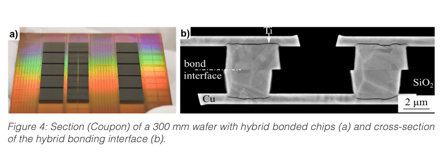
- High-density mixed-pitch interconnections based on hybrid bonding (Figure 4) and microbumps to enable bandwidths above 1 TB/s/mm2 according to UCIe-A and UCIe-3D.
Multi-Material Sensors (MMS) One platform, many sensors: The case for a universal silicon interposer The MMS demonstrator of the APECS pilot line integrates GaN gas sensing, acoustic CMUT, opto-chiplets and high-resolution magnetic Hall-arrays on a reusable interposer – a modular approach that lowers barriers for sensor development across industry.
The problem worth solving
Sensors rarely exist in isolation. In practice, whether for industrial monitoring, medical diagnostics or environmental analysis, useful sensing systems need to detect more than one quantity, often using different physical or chemical principles. The technologies behind these sensors, gallium nitride, silicon MEMS, photonic waveguides, capacitive transducers, magnetic Hall structures, come from very different material and process environments. Today, integrating them into one system almost always means starting the packaging design from scratch.
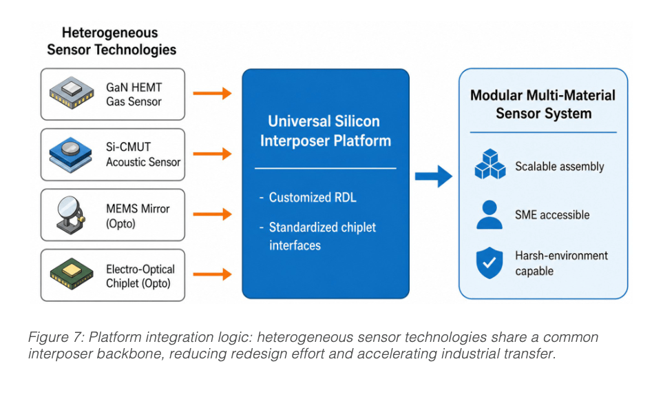
The MMS demonstrator within the APECS pilot line is a direct response to that problem. Its goal is not to develop one new sensor, but to show that a common silicon interposer infrastructure can serve as the integration backbone for several sensor technologies simultaneously, and that this approach can work at an industrially relevant scale.
A platform, not a package
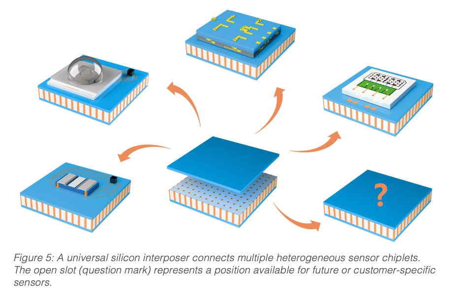
At the centre of the MMS concept is a silicon‑based interposer with a universal core design. This is the component that all sensor chiplets are built around. The interposer features very deep through‑silicon vias in the range of 300 to 400 µm. What makes the platform reusable is the redistribution layer (RDL): rather than designing a new interposer for each sensor combination, only the RDL is adapted to the specific interface geometry and signal requirements of the respective chiplet.
This separation of stable backbone and adaptable interface is what the APECS team refers to as a System-Technology Co-Optimization (STCO) approach. All sensor chiplets must comply with a defined interface standard. The analogy is closer to a standardized connector system than to a conventional custom package, and it has direct consequences for how quickly new technologies can enter the platform and reach industrial use. The open slot with the question mark in the interposer figure is therefore more than a graphic element, it is intended to indicate that additional sensors can be added to the same backbone.
Four sensor families, one platform
The MMS demonstrator currently integrates four distinct sensor technologies, each representing a different application domain. The first is a GaN‑based HEMT hydrogen gas sensor designed for operation in harsh environments. A GaN‑on‑Si/QST sensor chip is heterogeneously integrated with a silicon readout IC on the interposer. GaN HEMT structures are well suited to this application because of their thermal stability and sensitivity to surface charge changes induced by gas adsorption. First chiplets from this sub‑demonstrator have already been fabricated, and the development target is the first 8‑inch European GaN sensor platform, which is intended to be accessible to SMEs.
The second technology is an acoustic sensor (Si‑CMUT). Several CMUTs are co‑packaged with a CMOS chip on a silicon pocket wafer using QMI technology, and the resulting chiplet is then mounted onto the common interposer. Preliminary process studies for this chiplet have been completed successfully. The chiplet makes the acoustic integration accessible to SMEs in the sensor market.
The third set of components is the opto‑chiplet, which consist of two separate devices. The first is a MEMS mirror based on an epi‑poly‑silicon device assembled in a hermetically sealed package with a glass interposer and a glass dome for optical
access. The second is an electro‑optical chiplet that uses post‑CMOS photonics: QMI technology allows photonic waveguides and circuits to be fabricated on top of a CMOS wafer after the transistor process is complete. Both chiplets are mounted onto the interposer using the same platform logic as the GaN and acoustic components.
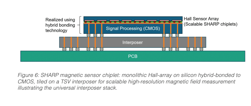
Another sub‑demonstrator is the SHARP concept (Silicon Hall‑Array High‑Resolution Platform), which is based on a monolithic three‑dimensional high-resolution Hall sensor array in silicon that is stacked onto a separate CMOS substrate for signal processing using hybrid wafer‑to‑wafer bonding. Each SHARP chiplet behaves as a self‑contained measurement system, but several chiplets can be placed side by side on the interposer to form a seamless, large‑area magnetic field sensor array. Typical application scenarios include magnetic field cameras, non‑destructive testing in mechanical engineering, and field homogeneity measurements.
Together, these four sensor families show that the MMS interposer is not tied to a single device type.
Why this matters and what it changes
The competitive argument for the MMS platform rests on a straightforward
observation: packaging design today is largely technology‑specific. A company that develops a GaN‑based device faces a different packaging workflow than one working with acoustic MEMS and combining both in one product typically means building a new assembly architecture from the ground up. Adding the opto‑chiplets or high‑resolution magnetic arrays make the situation even more complex. This is slow, expensive and creates a structural disadvantage for smaller players who lack the resources to repeatedly qualify new packaging processes.
The MMS interposer concept addresses this at the architecture level. By defining a common interface standard and a reusable core design, it allows new sensor chiplets to enter the platform without triggering a full system redesign. The question‑mark slot in the interposer figure is the practical expression of this: it is a real integration position, not a placeholder, and it is meant to communicate to industrial partners that the platform is open for extension.
Finally, the APECS approach is explicit about supply‑chain accessibility. The demonstrator work includes interface standardization and supply‑chain coordination across all sub‑demonstrators, with the specific aim of making the platform usable by SMEs. The first 8‑inch GaN sensor platform being developed within the HEMT sub‑demonstrator carries this intent directly: it is designed from the start to be available to companies that do not have in‑house access to GaN wafer‑scale processing. The chiplet format of the CMUT, opto‑ and SHARP modules follows the same logic, advanced sensor functions are provided as standardised building blocks that can be combined on the interposer without each
user having to develop their own process
chain.
Taken together, the MMS demonstrator of the APECS pilot line shows that heterogeneous sensor integration does not require a different approach for every material class. A well-designed interposer platform with standardized interfaces and an adaptable redistribution layer can serve as the shared infrastructure for GaN, acoustic, opto-chiplets and magnetic Hall array technologies simultaneously. The result is a modular sensor system platform that reduces integration complexity, shortens time to market and opens advanced packaging to a broader industrial user base.
Photonic integration (PI)
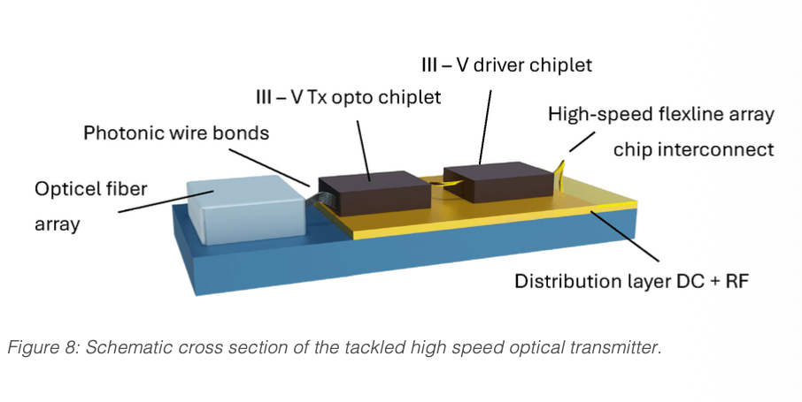
With the Photonic Integration demonstrator, APECS pilot line’s capability regarding hybrid-integration of III-V opto chiplets with III-V electronic chiplets will be demonstrated: A high speed 1300nm InP based Electro- absorption Modulated Laser (EML) 4 channel array will be hybridly integrated with an InP based DHBT driver chiplet on a common based interposer including all electrical high-speed connections and coupling to an optical fiber array. Target is to achieve a 1300nm 4 x 200Gbps PAM4 transmitter (schematic view see Figure 8)
A comprehensive transmitter hybrid integration concept was developed, based on a Si-based interposer that hosts the EML
4-array chiplets, the InP driver chiplets, and the associated highfrequency RF feeding lines. This interposer will be cointegrated with a fiberarray unit on a suitable heat dissipative submount. The required metallization and insulation layers have been defined and currently work focusses on the detailed RF line layout and the mounting and alignment processes and sequence for the implementation of EML, driver chiplet and fiber array.
A major achievement of the first project year is the reduction of the InP EML 4-array pitch from 640 µm to 375 µm, significantly increasing the shoreline density while simultaneously improving device performance: the EML modulation speed could be increased from 200 Gbps PAM4 to 290 Gbps PAM4. The achieved shoreline density currently is a record value for such EML 4-arrays. The final target in APECS is to achieve a pitch of 250 µm only.
Progress was also achieved on the InP DHBT driver chip, which now reaches an electrical bandwidth of more than 160 GHz. Further speed improvements are planned.
The optical interface between the EML 4-array and the fiber 4-array was further advanced, with the first successful demonstration of multichannel optical coupling using photonic wire bonds, a key enabler for alignment-tolerant coupling and for bridging disparate modefield diameters. The PI-Demonstrator transmitter represents an example for the hybrid integration of III-V optoelectronic components on a common interposer inclusive fiber coupling. The developed technology will pave the way for the future realization of customized hybridly integrated photonic and electronic chiplets within the APECS pilot line.
Radio frequency integration (RF)
The RF integration demonstrators will showcase the potential of the APECS pilot line in the field of complex, highly integrated RF systems up to 325 GHz. The performance and innovative potential of various combinations
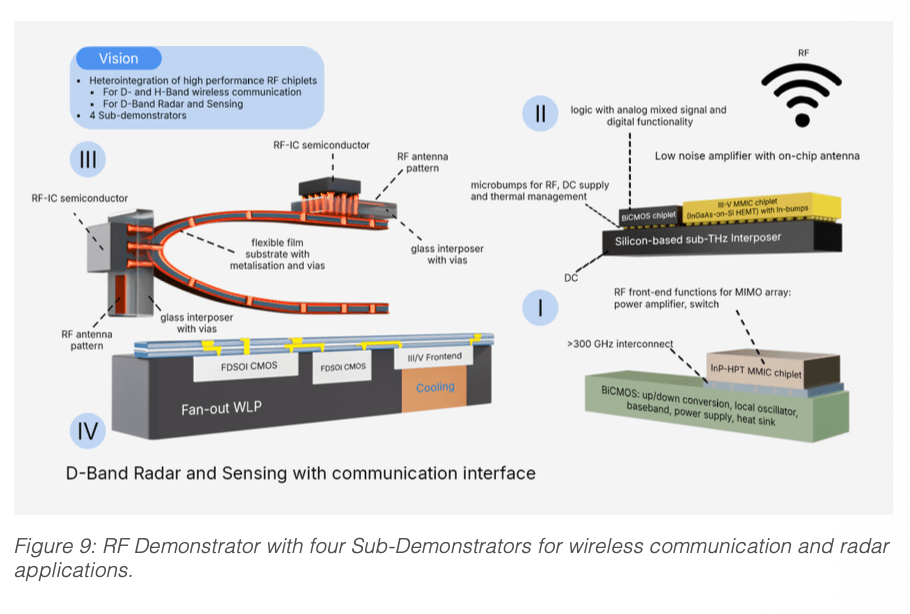
of semiconductors and heterogeneous integration technologies will be demonstrated. The applications addressed range from next-generation high data-rate mobile communications and wireless links to advanced radar and sensing systems.
Besides the various possible combination of advanced semiconductors by innovative heterogenous integration technologies, four RF technology demonstrators, as shown in Figure 9, will be realized: a InP-on-BiCMOS TRX: 6G D-Band Transceiver (1.), a Sub-THz BiCMOS-mHEMT Transceiver on Interposer (2.), a Flex D-Band Radar (3.) and a D-Band Communication Module (4.).
- InP-on-BiCMOS TRX: 6G D-Band Transceiver
The D-band (110…170 GHz) offers large absolute bandwidth for wireless
communications as needed, e.g., for high-data rate point-to-point links in the backhaul network of 5G and 6G base stations. The heterogeneous integration of high performance SiGe BiCMOS chiplets together with bipolar InP chiplets will boost output power and efficiency at D-band, thus extending range and energy efficiency. The different building blocks and subcircuits of a transceiver will be partitioned between the SiGe- BiCMOS and the InP-HBT technologies considering the best performance of each individual technology to maximize the overall system performance. The approach provides the seamless integration of the two technologies with high performance and broadband interconnects using microbumps. - Sub-THz BiCMOS-mHEMT Transceiver on Interposer
The Sub-THz BiCMOS-mHEMT Transceiver on Interposer demonstrator targets the heterogeneous integration of sub-THz chiplets and interposer technologies for high-resolution sensing above 200 GHz. The demonstrator aims to realize a high resolution FMCW radar frontend operating at 256 GHz by combining a SiGe BiCMOS transceiver chiplet together with InGaAs mHEMT amplifier chiplets on a common interposer platform. Glass and silicon interposers together with various flip chip interconnection technologies are applied to enable high-performance interconnects at such high frequencies. In summary, a scalable, low loss, compact and modular platform for sub-THz systems-on- interposer for sensing applications will be demonstrated.
- Flex D-band radar
Compared to sub-demonstrators 1. and 2., the Flex D-band radar will be a remarkable testcase of the pilot line’s capabilities in integrating a multi-module radar system onto bendable and/or non- planar surfaces. The concept is based on a heterogeneously integrated D-band (110 – 170 GHz) radar transceiver mounted on an RF-glass interposer using flip-chip technology. In addition, broadband TX and RX antennas will be implemented directly on the RF-glass interposer and connected to the radar chiplet via low-loss interconnects. This approach offers significant advantages over on-chip antennas, including higher efficiency and wider frequency bandwidth. These radar modules – each consisting of a D-band frontend and an RF-glass interposer with an antenna array – will be integrated multiple times onto a flexible polymer interposer. The resulting innovation is a multi-module radar system that is well suited for integration into or onto bendable and/or non-planar surfaces, such as the wings of wind turbines or drones or moving robot arms to give just a few examples. - D-band communication module
In alignment with sub-demonstrator 3. above, the sub-demonstrator 4. is also guided by the goal to show the integration of multiple chiplets. Here, a fan-out wafer level packaging (FOWLP) approach will be presented. FOWLP is well suited for RF and mmWave application due to shortest interconnects and feasibility of passive components and structure integration. The package will co-integrate two technologies: gallium nitride (GaN) and advanced FDSOI CMOS. Also cooling structures are integrated to ensure long- term stability of the integrated chiplets.
For each RF sub-demonstrator, the STCO (System-Technology Co-Optimization) process is used to achieve the highest possible system performance within a short development timeframe for highly integrated RF systems that combine different integration and semiconductor technologies. Within the APECS framework, this requires very close collaboration between Design and Design Enablement, as well as with semiconductor and integrations Technologies and the characterization, test and reliability capabilities and experts. In this sense, the demonstration projects are also the first “customers” to use the STCO and to conduct a proof-of-concept for the STCO.
Dr. Dirk Schumann

Dirk Schumann studied physics in Berlin and earned a doctorate in semiconductor physics. With over 30 years in the semiconductor and automotive sectors, he has held technology-driven leadership roles across Germany and Europe. Since June 2025, he leads the APECS project, focusing on industrializing and commercializing advanced technologies.