

Written by Richard Hall-Wilton / Director of Sensors&Devices / Zahra Bisadi – Project Manager / Sensors&Devices Centre at Fondazione Bruno Kessler / FBK / Published on September 15, 2026
Europe’s ambition to strengthen its technological sovereignty in semiconductors depends on one critical challenge: transforming cutting-edge research into scalable industrial innovation. At Fondazione Bruno Kessler’s Sensors and Devices Centre (FBK-SD), this transition is becoming a reality through a strategic combination of European initiatives, including IPCEI ME/CT and the Chips JU Pilot Lines. These flagship programmes are not only expanding FBK’s research and technological capabilities but are also creating an innovation ecosystem where advanced semiconductor technologies can move efficiently from laboratory development to industrial deployment.
Building on decades of expertise in silicon sensors, micro- and nanofabrication, FBK is investing in next-generation platforms based on silicon carbide, silicon-germanium and 3D integration, supported by new cleanroom infrastructure and an open innovation model designed to foster collaboration with industry; this supports a vibrant lab-to-fab model. From high performance sensors and MEMS for space, healthcare, environmental monitoring and autonomous systems to pilot manufacturing capabilities that accelerate technology transfer, these European projects demonstrate how coordinated investments in research infrastructures can bridge the gap between scientific excellence and market-ready solutions, reinforcing Europe’s competitiveness in the semiconductor value chain.
Building the foundations of Europe’s semiconductor future
The FBK Sensors and Devices Centre is built around a core mission of advancing sensor technology and achieving market adoption of the technologies. The centre has around 200 staff members including researchers, technologists, technicians, PhD students and interns. Its micro- and nano- facility, extending over 2000 sqm, is ISO 9001 and 27001 certified. The facility consists of 5 cleanrooms: CRD – silicon detectors, CRM
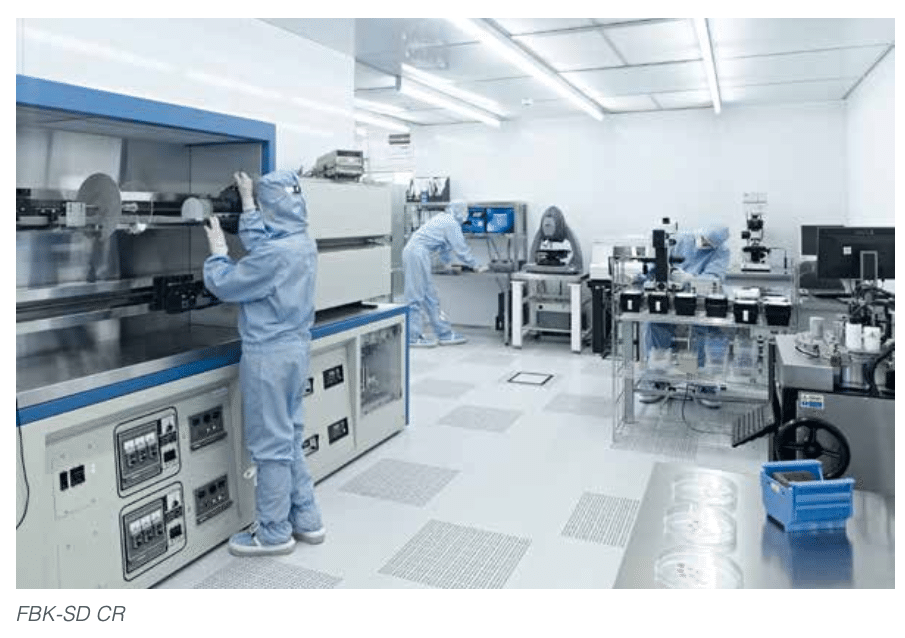
– MEMS and NEMS, CRP – packaging and integration, CR3D – 3D integration, and CRSiC – SiC deposition (around 600 sqm currently under construction, thanks to IPCEI ME/CT). The cleanroom facility itself has been talked about in detail in issue 10 of the July 2025 issue of INSIDE Magazine.
With a decadal investment budget of around 100 million euro, FBK-SD is participant in IPCEI ME (closed in June 2025), IPCEI ME/CT, and 4 Chips JU Pilot Lines: Wide Bandgap (WBG), PIXEurope, SUPREME and DIREQT.
IPCEI ME/CT is a collaborative initiative aimed at driving innovation, research, and industrial deployment across the microelectronics and communication technologies value chain. Led by fourteen Member States of the European Union, this project represents a strategic endeavor to foster digital and green transformation while enhancing Europe’s competitiveness in key sectors
Utilising the technologies built on the success of the IPCEI ME project, the Centre is actively driving its proprietary R&D roadmap within IPCEI ME/CT Sense Workstream, focused on advancing microelectronics technologies to produce advanced sensing systems that feature high precision, low energy consumption, embedded intelligence, sensor fusion capabilities, and high reliability applicable to various sectors, ultimately supporting Europe’s technological and industrial leadership in semiconductors development.
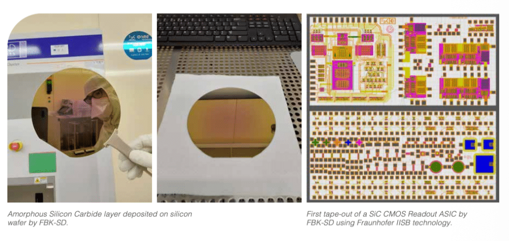
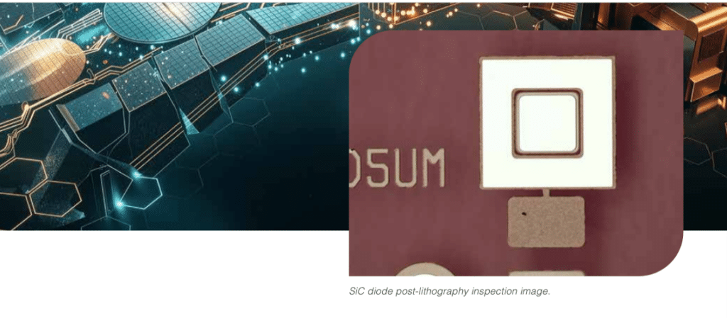
In IPCEI ME, FBK-SD developed the 3D integration platform applied to SiPM (Silicon photon multipliers) and SPAD (Single-Photon Avalanche Diode) technologies and in IPCEI ME/CT, it is extending its micro- and nano-fabrication capabilities – both infrastructure and equipment – to Group IV semiconductors other than silicon, particularly SiC, as well as to develop new hetero-integration capabilities to provide advanced silicon-on-chip/silicon- on-package solutions. Silicon carbide has well-known advantages for power electronics; these advantageous properties can also be key in advancing sensor technology and capability, though silicon carbide sensors are at a very nascent stage of research currently. During the first two years of the project, significant progress has been achieved in establishing SiC technologies. Our team successfully deposited amorphous SiC on silicon substrates and completed the first tape-out of a SiC CMOS readout ASIC using Fraunhofer IISB technology.
Experimental results from the amorphous SiC deposition and surface characterisation closely matched theoretical predictions, confirming the validity of the developed approach. The project has also strengthened collaboration with European suppliers,
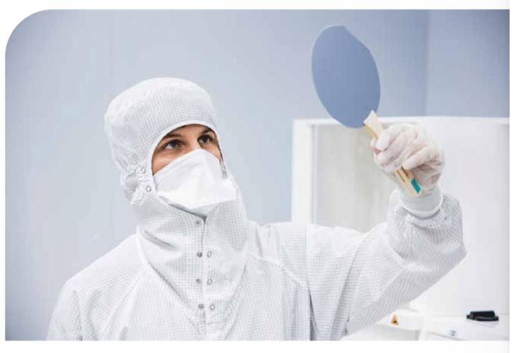
supporting both the procurement of advanced equipment, the co-development of a SiC processing system and material evaluation as part of process research.
Accelerating the path from research to industrial impact
FBK is playing a key role in Europe’s effort to strengthen its semiconductor ecosystem through its participation in four Pilot Lines co-funded by the Chips JU. Access to pilot, small and medium fabrication capacity is the main barrier to market entry of novel devices. These large-scale European initiatives are designed to bridge the gap between research and industrial manufacturing, accelerating the uptake of strategic semiconductor technologies while reinforcing Europe’s technological sovereignty, innovation capacity, and supply chain resilience. By contributing its expertise in micro- and nano-fabrication, photonics, quantum technologies, and advanced materials, FBK is helping transform cutting-edge research into manufacturing-ready solutions for the next generation of electronic and quantum devices.
As part of the WBG PL consortium, FBK is contributing to the development of wide bandgap (WBG) semiconductor technologies specifically for non-power applications. FBK is realising advanced sensor technologies particularly for harsh chemical, physical, high temperature, or radiation environments, and RF-MEMS electronics. It is also looking at SiC waveguides as part of its photonic integrated circuits in the NIR-VIS regime, and defect engineering in silicon carbide for quantum and photonic applications. By strengthening the capabilities of the participating pilot-line facilities, the initiative addresses key front-end manufacturing challenges and enables the development of high-performance devices that surpass the limits of conventional silicon technologies.
Within PIXEurope, FBK-SD joins 19 other institutions from 11 European countries to establish a globally unique Open Access Pilot Line for Photonic Integrated Circuits (PICs). The project addresses critical technological and manufacturing challenges while supporting RTOs and industry in accelerating the transition from laboratory innovation to industrial production.
As a partner in the quantum pilot line SUPREME, the SD Centre is helping bridge the gap between cutting-edge research and industrial-scale manufacturing of superconducting quantum technologies. Through pre-commercial fabrication services for superconducting quantum devices, the pilot line enables researchers and companies to design, prototype, and validate innovative solutions using advanced, standardised manufacturing processes, accelerating their path towards market-ready applications.
FBK is also contributing to DIREQT, the European pilot line dedicated to diamond quantum technologies. Covering the entire diamond value chain, the initiative aims to transform laboratory advances into scalable manufacturing, paving the way for the large-scale production of diamond quantum chips and supporting the emergence of a competitive European quantum ecosystem.
In summary
The adage of the enthusiastic investigative journalist is “follow the money”; this is very apt for the deeptech semiconductor ecosystem too, where huge investments are needed to realise technological progress. As shown above, the current investments in IPCEI ME/CT and in the Chips JU Pilot Lines are enabling future products to bridge the gap between research and industrial deployment, mediated by research and technology organisations with a specific remit in applicative development. This investment level needs to be sustained and intensified if
the ambition for Europe to produce a higher fraction of its own chips is to be realised. Similarly, there is a contrast between the speed of research and that of the semiconductor market; again, this is best bridged by RTOs with a focus on getting novel innovation out there in the market.